The SX1308 Module is a adjustable DC to DC step up power boost converter circuit, which can convert 2-24V input to 2-28V output at a 95% efficiency rate, using 1.2 MHz switching frequency, and capable of delivering a maximum output current of 2A.
The device has impressive efficiency with its compact design, featuring tiny, low-cost capacitors and an inductor measuring 2mm or less in height, which results in a small inrush current and extends battery life.
Additionally, its internal soft-start ensures smooth operation, while the automatic shifting to pulse frequency modulation mode at light loads further enhances its energy-saving capabilities.
These module price typically ranged from $0.4 to $1, depending on the supplier and quantity purchased. It's always a good idea to compare prices from different suppliers to find the best deal.
This article will provide detailed information about SX1308 step-up converter module, including specifications, circuit diagrams, working principle, applications, and more. Let's get started!
SX1308 Module Specifications
The quick specifications of the SX1308 module are given below:
- Type: Adjustable Boost Converter
- Model: SX1308
- Input Voltage: DC 2-24V
- Output Voltage: DC 2-28V
- Maximum Output Current: 2A
- Switching Frequency: 1.2MHz
- Operating Temperature: -40°C to +85°C
- Efficiency: 95%
- Dimensions: 24 x 16 x 7 mm
- Weight: 6gm
SX1308 Module Circuit Diagram
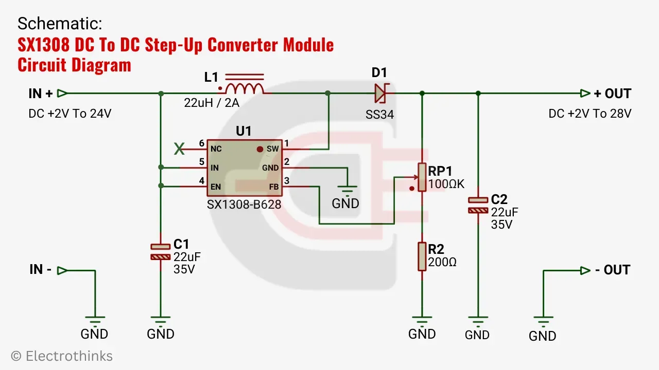
Schematic of the SX1308 dc to dc step-up converter module circuit is shown below.
Components are used in the circuit - U1: SX1308-B628 IC, RP1: 100KΩ Multiturn Potentiometer, R2: 200Ω Resistor, D1: SS34 Schottky Diode, C1 & C2: 22µF 35V Electrolytic Capacitor, and L1: 22µH Inductor.
Working Principle of SX1308 Module
The working principle of the SX1308 module circuit is simple, with the main component being the SX1308 6-pin B628 integrated circuit.
According to the functional block diagram, the IC (U1) has an error amplifier, PWM comparator, control logic, integrated 80mΩ power MOSFET, current sense amplifier, and OSC.
When the boost converter module receives the input DC supply, capacitor (C1) is charged. Initially, the IC (U1) starts switching and current is passed through inductor (L1) directly from the input source, inducing a magnetic field.
The IC (U1) uses a fixed 1.2MHz frequency peak current mode booster architecture to regulate the voltage at feedback pin-3 and change the current level passing through (L1).
Therefore, during the IC turn-on stage, the magnetic field collapses, generating a high voltage spike. When the IC turns off stage, the voltage spike passes through Schottky diode (D1), which blocks reverse current to the circuit and stores the power in capacitor (C2).
This increases the voltage of capacitor (C2), and the output obtains a higher voltage level across the capacitor, up to 28 volts.
The output is controlled through potentiometer (RP1) and resistor (R2) voltage divider setup, which easily adjusts to the required output voltage level.
SX1308 Module Applications
- LCD Bais Supply
- Battery-Powered Equipment
- Digital subscriber line, Cable Modems and Routers
- Set-Top Boxed
- Networking cards powered from PCI express slots


No comments
If you have any doubts or questions, please let me know. Don't add links as it goes to spam. Share your valuable feedback. Thanks