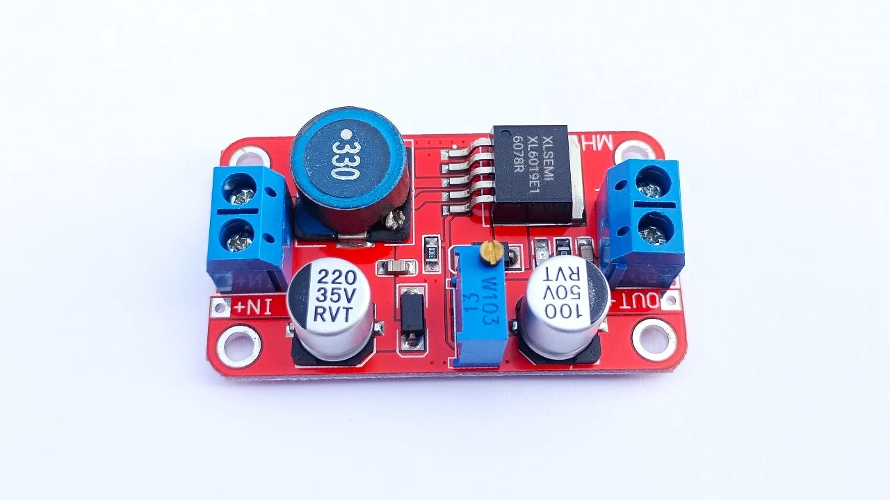
The XL6019 module is a adjustable DC to DC 30W power boost converter circuit board, which can convert the input DC 3-35V to DC 5-40V output at a 97% efficiency rate, using 220 kHz switching frequency, and capable of delivering a maximum output current of 5 Amp.
Here, I will discuss and explain the workings of this compact adjustable DC-DC step-up converter along with its circuit diagram.
XL6019 Module Specifications
The quick technical specifications of this boost converter module are given below.
| Type | DC-DC Voltage Boost Converter |
| IC Used | XL6019E1 (TO263-5) |
| Input Voltge | DC 3V to 25V |
| Input Current Max. | 5A |
| Output Voltage | DC 5V to 40V (Adjustable) |
| Output Power Max. | 30W |
| Output Ripple Max. | 100mV |
| Conversion Efficiency | 97% |
| Frequency Range | 220kHz |
| Working Temperature | Industrial (-40 °C to +85 °C) |
| Dimensions (L X W X H) | 50 X 28 X 13mm |
Working Principle of XL6019 Module Circuit
Schematic of the xl6019 adjustable d.c. to d.c. step up converter circuit is shown below.
Components are used in the circuit - U1: XL6019E1 IC, D1: M7 SMD Diode, C1: 220uF 35V SMD Aluminum Electrolytic Capacitor, C2 & C3: 1uF (105) Ceramic Capacitor, L1: 33uH (330) Inductor Resistor, D2: SS34 Schottky Power Diode, C4: 100uF 50V SMD Aluminum Electrolytic Capacitor, PR1: 10kΩ Multiturn Variable Resistor, R1: 330Ω (3300) Resistor, R2: 1kΩ (102) Resistor, and D3: SMD LED.
| PCBWay Custom PCB Service!!! You can start ordering a PCB for Only $5 and explore more discounts and special offers for PCB fabrication and assembly services. 👇 |

|
The working principle of the XL6019 adjustable DC to DC step up converter circuit is simple. The main component 5-pin XL6019E1 TO263-5 IC (U1) has an error amplifier, soft start, integrated reference 1.25V, OVLO, OVP, PWM comparator, RS latch, integrated 80mΩ power MOSFET with driver, thermal sense, and OCP.
The input DC supply charged the capacitor (C1) through series setup of inductor (L1) & Schottky diode (D2). The diode (D1) is placed in reverse bias to prevent reverse polarity input voltage.
Initially, the Vin pin (4) of the IC (U1) receives the input DC supply and starts ~220kHz switching through its SW pin (3) and current (5A max.) is passed through inductor (L1) directly from the input DC source. SW is the drain of the internal MOSFET switch and swing between GND and 3-25V.
IC's EN pin (2) is On/Off control input, which is usually connected to the input supply for automatic startup.
During the IC turn-on stage, it inducing a magnetic field in the inductor, generating a high voltage spike. In the IC turn-off stage, the voltage spike passes through diode (D2), which blocks reverse current to the circuit and increases the voltage of capacitor (C3), up to 40 volts. To remove the noise in voltage a ceramic resistor (C2 & C3) is used dedicetly in input/output of the converter.
The output voltage is controlled through a multiturn variable resistor (PR1) and fixed resistor (R1) voltage divider setup, which is reffering a 1.25V signal voltage to the IC FW pin (5). The internal control logic easily adjusts to the required output voltage level and continously mainting the set voltage in a load condition.
XL6019 Module Applications
- 3V7/5V to 12V Buck-Boost.
- LED Driver - up to 30 Watts.
- Adjustable DC-DC Power Supply.
- Portable Electronic Equipment.


No comments
If you have any doubts or questions, please let me know. Don't add links as it goes to spam. Share your valuable feedback. Thanks