A peak detector is an electronic circuit designed to identify and hold the highest value (peak) of an input signal. This function is crucial in various applications such as signal processing, communications, and instrumentation. Peak setectors are commonly used in systems that require the measurement of peak amplitudes, like oscilloscopes, audio equipment, and RF signal processing. Here designed a peak detector using an Op-Amp LM741 and some discrete components, which makes it a useful, and portable solution.
Components List
The following components are required to make this diy peak detector:
- U1: LM741 Op-Amp IC - 1 pcs
- R1, R2: 10kΩ 1/4W Resistor - 1 pcs
- D1: 1N914 Diode - 1 pcs
- C1: Ceramic capacitor between 0.1uF to 1uF - 1 pcs
- SW1: Tactile Switch 6X6x5MM - 1 pcs
- P1, P2, P3: 2-Pin Screw terminal connector - 3 pcs
Peak Detector Circuit Diagram
The schematic of a peak detector circuit using LM741 op-amp is shown below.

The working principle of the peak detector circuit is simple where the main component is the popular general-purpose operational amplifier LM741 (U1). The complete Technical Details can be found in the LM741 datasheet .
The input supply voltage of the circuit is +9V DC. The comparator IC charges the C1 capacitor positively due to the D1 diode until the voltage across the capacitor equals the input signal voltage. A push button (SW1) can be used to reset the circuit. The resistor R2 eliminates the DC offset caused by the op-amp input bias current. If the subsequent input voltage exceeds that stored in C1, the comparator voltage will go high and charge C1 to the new higher peak voltage, thus detecting every peak of the input signal voltage.
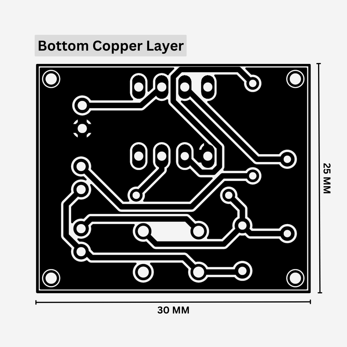
Peak Detector PCB Design
Assemble the circuit on a PCB as it saves time and minimizes assembly errors. An actual-size, single-side PCB with component layout for the peak detector circuit is shown below. Carefully assemble the components and double-check for any overlooked errors.

|

|
| Peak Detector PCB Layout. | A PCB for the peak detectore circuit. |


No comments
If you have any doubts or questions, please let me know. Don't add links as it goes to spam. Share your valuable feedback. Thanks