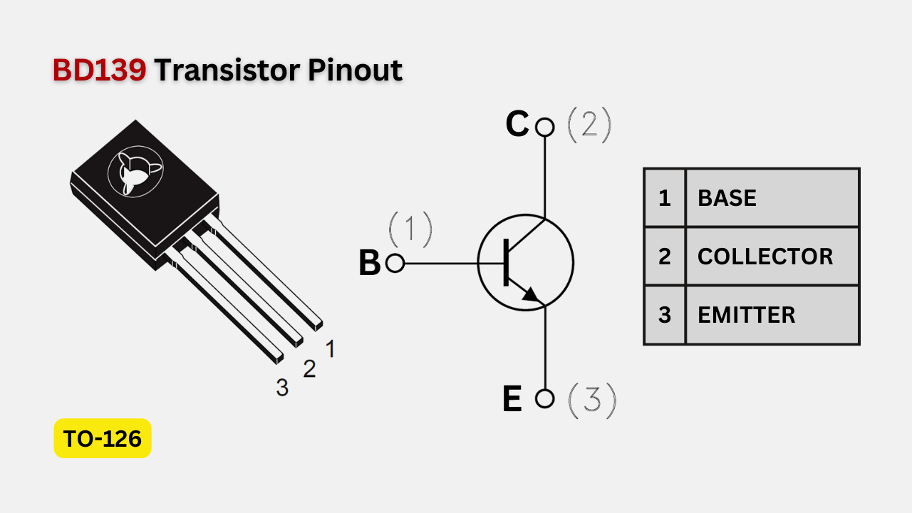
The BD139 is a silicon NPN transistor and housed in a TO-126 package suitable for medium-power tasks in switching and amplification.
It can handle up to 80V for collector-base and collector-emitter voltages, with a maximum collector current of 1A. The emitter-base voltage is 5V, and this transistor can dissipate up to 12W of power. With a minimum Beta (β) of 40, the BD139 transistor ensures reliable performance across various applications.
2SD882 Pinout Configuration

The pin configuration of the BD139 transistor is as follows:
| Pin No. | Name | Description |
|---|---|---|
| 1 | Emitter | Electrons emitted from the emitter into the first PN. |
| 2 | Collector | Electrons Emitted from Emitter Collected by the Collector. |
| 3 | Base | Controls the biasing of the transistor. |
Absolute Maximum Ratings of BD139
The quick technical specifications and features of the bd139 transistor are given below:
- Transistor Type: Si
- Polarity: NPN
- Emitter-Base Voltage (Veb max.): 5V
- Collector Power Dissipation (Pc max.): 12W
- Collector-Base Voltage (Vcb max.): 80V
- Collector-Emitter Voltage (Vce max.): 80V
- Collector Current (Ic max.): 1A
- Operating Junction Temperature (Tj): -55°C to 150°C
- Transition Frequency (ft): 50MHz
- Forward Current Transfer Ratio (hFE min.): 40
- Noise Figure (dB): -
- Package: TO-126
Note: Complete Technical Details can be found in the BD139 transistor datasheet given at the end of this page.
BD139 PNP Complementary
The BD140, BD140G, BD140-6 medium power bipolar PNP transistors are the complementary transistor of the BD139.
BD139 Equivalent Transistor
| Transistor | Type | Polarity | Pc | Vcb | Vce | Veb | Ic | Tj | Ft | Hfe | Caps |
|---|---|---|---|---|---|---|---|---|---|---|---|
| BD139G | Si | NPN | 12 | 80 | 80 | 5 | 1 | 150 | 50 | 40 | TO126 |
| BD139-6 | Si | NPN | 12 | 80 | 80 | 5 | 1 | 150 | 50 | 40 | TO126 |
These two transistors have similar features and can be used as replacements for the BD139 in terms of their package, emitter-base voltage, transition frequency, and forward current transfer ratio. But there might be slight differences in pin layout. Please verify before using them in a PCB or project.
Applications of BD139
- Switching load of up to 1A
- Audio Amplifiers
- LED drivers
- Motor control
- Power supplies
- Electrical signals
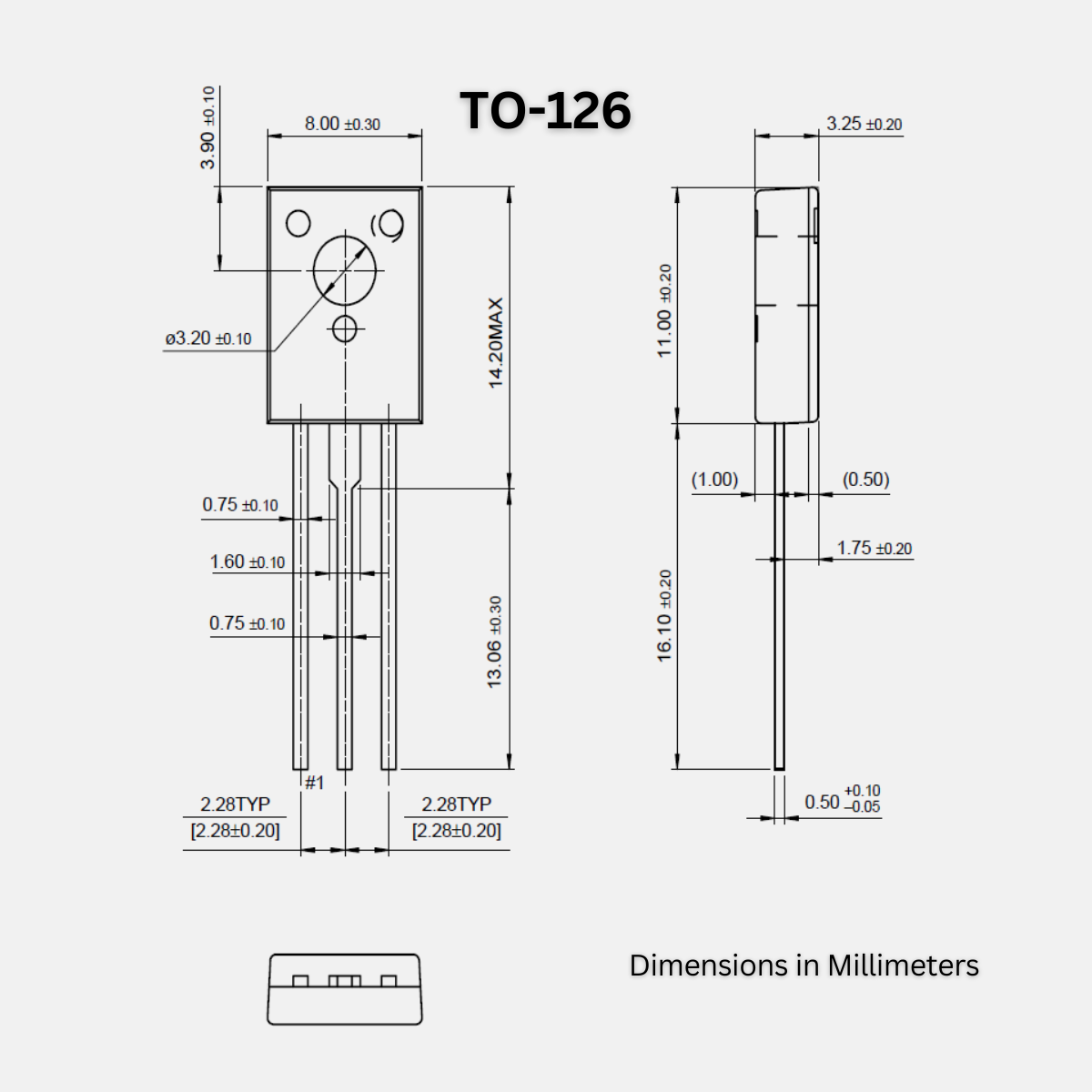
BD139: 2D Model and Dimensions
If you are designing a PCB or perf board with this component, the following picture from the BD139 datasheet will be useful to determine its package type and dimensions.

BD139 Safe Operating Guidelines
It is recommended not to push the BD139 transistor to its absolute limits. It's best to stay at least 20% below its maximum ratings. For example, while it can handle a maximum load of 1A, it's safer to avoid exceeding 800mA. Similarly, its maximum load voltage is 80V, so it's advisable to stay below 64V. Additionally, ensure the transistor's temperature stays between -55°C and +150°C for proper operation.


No comments
If you have any doubts or questions, please let me know. Don't add links as it goes to spam. Share your valuable feedback. Thanks